- 您现在的位置:买卖IC网 > Sheet目录1998 > ICS8741004AGLFT (IDT, Integrated Device Technology Inc)IC PCI EXPRSS/JITT ATTEN 24TSSOP
ICS8741004
DIFFERENTIAL-TO-LVDS/0.7V DIFFERENTIAL PCI EXPRESS JITTER ATTENUATOR
IDT / ICS PCI EXPRESS JITTER ATTENUATOR
12
ICS8741004AG REV. AMAY 29, 2008
Recommendations for Unused Input and Output Pins
Inputs:
LVCMOS Control Pins
All control pins have internal pull-ups or pull-downs; additional
resistance is not required but can be added for additional
protection. A 1k
resistor can be used.
Outputs:
Differential Outputs
All unused differential outputs can be left floating. We recommend
that there is no trace attached. Both sides of the differential output
pair should either be left floating or terminated.
LVDS Outputs
All unused LVDS output pairs can be either left floating or
terminated with 100
across. If they are left floating, we
recommend that there is no trace attached.
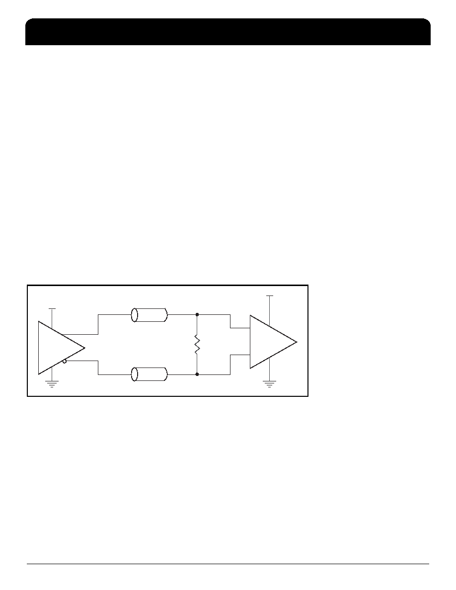
LVDS Driver Termination
A general LVDS interface is shown in Figure 4. In a 100
differential transmission line environment, LVDS drivers require a
matched load termination of 100
across near the receiver input.
For a multiple LVDS outputs buffer, if only partial outputs are used,
it is recommended to terminate the unused outputs.
Figure 4. Typical LVDS Driver Termination
3.3V
LVDS Driver
R1
100
–
+
3.3V
50
50
100
Differential Transmission Line
发布紧急采购,3分钟左右您将得到回复。
相关PDF资料
ICS87604AGILF
IC CLK MULT/ZD BUFFER 28-TSSOP
ICS8761CYLFT
IC CLK GEN PCI/PCI-X 64-LQFP
ICS87946AYILFT
IC CLOCK GENERATOR 32-LQFP
ICS87949AYILFT
IC CLOCK GEN LVCMOS 52-LQFP
ICS87950BYILF
IC CLK MULT LVCMOS/LVTTL 32-LQFP
ICS87952AYI-147LF
IC CLK MULT/ZD BUFFER 32-LQFP
ICS87972DYI-147LF
IC CLK MULT/ZD BUFFER 52-LQFP
ICS87973DYI-147LF
IC CLK MULT/ZD BUFFER 52TQFP
相关代理商/技术参数
ICS8741004BGILF
功能描述:IC PCI EXPRSS/JITT ATTEN 24TSSOP RoHS:是 类别:集成电路 (IC) >> 时钟/计时 - 专用 系列:HiPerClockS™, FemtoClock™, PCI Express® (PCIe) 标准包装:1,500 系列:- 类型:时钟缓冲器/驱动器 PLL:是 主要目的:- 输入:- 输出:- 电路数:- 比率 - 输入:输出:- 差分 - 输入:输出:- 频率 - 最大:- 电源电压:3.3V 工作温度:0°C ~ 70°C 安装类型:表面贴装 封装/外壳:28-SSOP(0.209",5.30mm 宽) 供应商设备封装:28-SSOP 包装:带卷 (TR) 其它名称:93786AFT
ICS8741004BGILFT
功能描述:IC PCI EXPRSS/JITT ATTEN 24TSSOP RoHS:是 类别:集成电路 (IC) >> 时钟/计时 - 专用 系列:HiPerClockS™, FemtoClock™, PCI Express® (PCIe) 标准包装:1,500 系列:- 类型:时钟缓冲器/驱动器 PLL:是 主要目的:- 输入:- 输出:- 电路数:- 比率 - 输入:输出:- 差分 - 输入:输出:- 频率 - 最大:- 电源电压:3.3V 工作温度:0°C ~ 70°C 安装类型:表面贴装 封装/外壳:28-SSOP(0.209",5.30mm 宽) 供应商设备封装:28-SSOP 包装:带卷 (TR) 其它名称:93786AFT
ICS874208BKILF
制造商:Integrated Device Technology Inc 功能描述:IC CLK BUFFER/DIVIDER 32VFQFN
ICS874208BKILFT
制造商:Integrated Device Technology Inc 功能描述:IC CLK BUFFER/DIVIDER 32VFQFN
ICS87421AMILF
功能描述:IC CLK GEN DIFF-LVDS 8-SOIC RoHS:是 类别:集成电路 (IC) >> 时钟/计时 - 时钟发生器,PLL,频率合成器 系列:HiPerClockS™ 标准包装:2,000 系列:- 类型:PLL 频率合成器 PLL:是 输入:晶体 输出:时钟 电路数:1 比率 - 输入:输出:1:1 差分 - 输入:输出:无/无 频率 - 最大:1GHz 除法器/乘法器:是/无 电源电压:4.5 V ~ 5.5 V 工作温度:-20°C ~ 85°C 安装类型:表面贴装 封装/外壳:16-LSSOP(0.175",4.40mm 宽) 供应商设备封装:16-SSOP 包装:带卷 (TR) 其它名称:NJW1504V-TE1-NDNJW1504V-TE1TR
ICS87421AMILFT
功能描述:IC CLOCK GEN LVDS 8-SOIC RoHS:是 类别:集成电路 (IC) >> 时钟/计时 - 时钟发生器,PLL,频率合成器 系列:HiPerClockS™ 标准包装:1,000 系列:- 类型:时钟/频率合成器,扇出分配 PLL:- 输入:- 输出:- 电路数:- 比率 - 输入:输出:- 差分 - 输入:输出:- 频率 - 最大:- 除法器/乘法器:- 电源电压:- 工作温度:- 安装类型:表面贴装 封装/外壳:56-VFQFN 裸露焊盘 供应商设备封装:56-VFQFP-EP(8x8) 包装:带卷 (TR) 其它名称:844S012AKI-01LFT
ICS8743004DKILF
功能描述:IC CLK BUFFER ZD PLL 40VFQFN RoHS:是 类别:集成电路 (IC) >> 时钟/计时 - 专用 系列:HiPerClockS™, FemtoClock™, PCI Express® (PCIe) 标准包装:1,500 系列:- 类型:时钟缓冲器/驱动器 PLL:是 主要目的:- 输入:- 输出:- 电路数:- 比率 - 输入:输出:- 差分 - 输入:输出:- 频率 - 最大:- 电源电压:3.3V 工作温度:0°C ~ 70°C 安装类型:表面贴装 封装/外壳:28-SSOP(0.209",5.30mm 宽) 供应商设备封装:28-SSOP 包装:带卷 (TR) 其它名称:93786AFT
ICS8743004DKILFT
功能描述:IC CLK BUFFER ZD PLL 40VFQFN RoHS:是 类别:集成电路 (IC) >> 时钟/计时 - 专用 系列:HiPerClockS™, FemtoClock™, PCI Express® (PCIe) 标准包装:1,500 系列:- 类型:时钟缓冲器/驱动器 PLL:是 主要目的:- 输入:- 输出:- 电路数:- 比率 - 输入:输出:- 差分 - 输入:输出:- 频率 - 最大:- 电源电压:3.3V 工作温度:0°C ~ 70°C 安装类型:表面贴装 封装/外壳:28-SSOP(0.209",5.30mm 宽) 供应商设备封装:28-SSOP 包装:带卷 (TR) 其它名称:93786AFT